Futaba ELW3501AA OLED Driver Board
Personal hardware project · Aug 2026
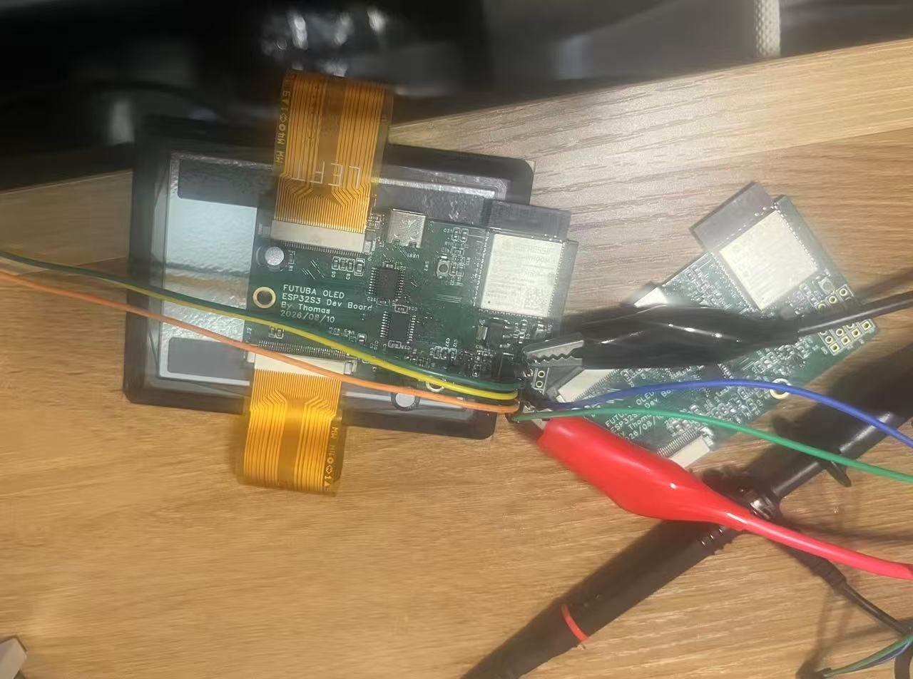
Designed and brought up a complete 6-layer controller for the Futaba ELW3501AA, a 3.5-inch, 228 × 168 passive-matrix OLED split across two driver ICs and two 40-pin FPCs. The finished ESP32-S3 system addresses both display halves over a 2 MHz i80 bus, renders 16-level grayscale test patterns through DMA, and applies the required rail and driver sequencing.
The project covered vendor-documentation reverse engineering, schematic capture, PCB layout, fabrication, assembly bring-up, ESP-IDF firmware, and hardware fault isolation. Full-panel operation was achieved after correcting the vendor reference pin mapping, replacing underspecified boost inductors, and tracing the remaining dark half to FPC contact. Brightness matching and full-white rail stability remain hardware follow-up items.
Display architecture
The panel exposes one master and one slave driver. Both share DB0–DB7, WR, RD, RS, and RESET, while CS1 and CS2 select the top and bottom 84-row halves independently. The PCB also carries the SCAN_EN, CLK2, and COMV bridge between the two FPC connectors so the master can provide scan timing to the slave.
Three rails must be sequenced: 5.0 V logic, 16.5 V VHA, and 12.9 V VHC. Display ON and OFF commands also have an inter-chip order requirement. Those constraints shaped both the power tree and the firmware state machine.
Board design and reference recovery
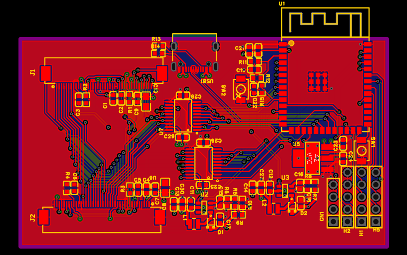
The board integrates an ESP32-S3-WROOM-1, two TXS0108E level shifters, dual SX1308 boost converters, two 40-pin FPC connectors, USB-C power, and bring-up headers. The eight data lines and control bus stay shared, while each display IC receives its own chip select and interrupt return.
During connector review, I found that the vendor reference schematic drew J1 mirrored while wiring it by visual position. That shifted every J1 signal by 21 pin positions in the supplied netlist. I rebuilt the mapping from the display pin table and checked both connectors in the final netlist pin by pin before fabrication.
ESP-IDF driver
One LCD_CAM i80 bus owns two esp_lcd panel-IO devices, one per chip-select line. A packed 4 bpp DMA-capable framebuffer stores all 228 × 168 pixels, then flushes either one half at a time or row by row to match the vendor access pattern.
The driver encodes the master/slave register differences, the 16-level grayscale table, RAM clear, and the mandatory power order. Because both boost converters share one enable pin, LEDC ramps that node from 5% to 100% duty over 300 ms to reduce USB inrush. Separate dry-run, CS square-wave, and INT frame-sync probes make power, transport, and scan failures distinguishable during bring-up.
Bring-up and fault isolation
The first illuminated test exposed a brownout and then an open VHA inductor. The fitted NLV25T-4R7J-PF was a 175 mA signal inductor, far below the boost converter current requirement. Replacing both boost inductors with low-DCR 4.7 µH power parts restored the 16.5 V and 12.9 V rails.
The top half then scanned while the bottom half stayed dark. Firmware calls completed successfully, so I followed the signal path instead of treating API success as proof: CS2 was checked through the level shifter to the connector, the master/slave bridge had continuity, and the INT probe measured 136 Hz on IC1 versus 0 Hz on IC2. Re-seating FPC2 restored both halves, identifying connector contact as the most likely cause.
The remaining brightness split and full-white flicker scale with illuminated area and are consistent with VHA/VHC load regulation, but that diagnosis was not closed with under-load rail measurements. A next revision should use a better-locating FPC connector; separate boost enables would also allow the two converters to start in sequence.
Engineering Timeline
Mapped the shared 8-bit i80 bus, independent chip selects, master/slave scan bridge, three power rails, and mandatory startup order from the vendor documentation.
Found the mirrored J1 drawing error in the reference design, rebuilt the FPC mapping from the display manual, and verified the final netlist pin by pin.
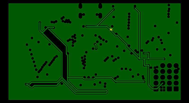
Completed routing, boost-loop placement, ground stitching, fabrication outputs, BOM, and pick-and-place data for JLCPCB assembly.
Brought up one shared LCD_CAM bus with two CS devices, DMA framebuffer flushes, register initialization, test patterns, and sequenced power control.
Separated USB inrush from the later hardware failure, found the 175 mA signal inductor open, and selected 4.7 µH power inductors using saturation current and DCR.
Used CS square-wave tracing, bridge continuity, and driver INT pulses to narrow the dark lower half to the FPC2 connection. Re-seating restored full-panel operation.
Highlights
- Designed and brought up a 6-layer ESP32-S3 driver board for a dual-controller 228 × 168 industrial passive-matrix OLED, achieving full-panel operation across both display halves
- Integrated 5 V level shifting and dual 16.5 V/12.9 V SX1308 boost rails, and corrected a mirrored FPC pin-mapping error in the vendor reference before fabrication
- Developed a 2 MHz ESP-IDF i80/DMA driver with dual-IC power sequencing, boost soft start, and frame-sync diagnostics that isolated power and FPC contact faults during bring-up